Lasers for Nanophotonics
Nanophotonics – or photonics at the nanoscale – is concerned with light-matter interactions that take place on the (sub-)wavelength scale, a domain where the nature of nanostructured matter controls the interactions.
This vast field of fundamental and applied research merges concepts of photonics with nanotechnology, i.e. with the multidisciplinary use of materials and processes at the nanometer scale. Nanophotonics holds great potential for enhancing the spatial resolution in imaging, creating new sensors with increased sensitivity and specificity, reducing the energies of device operations, and creating densely integrated information systems with lower power dissipation.
The characteristics of photonic nanostructures are often directly linked to the effect of so-called quantum-confinement. Depending on whether the confinement is one-, two-, or three-dimensional, the artificially created materials are referred to as Quantum Wells, Quantum Wires (with Carbon Nanotubes considerably the most prominent example), or Quantum Dots, respectively. The spectroscopic characterization of such systems frequently requires excitation laser tuning throughout a wide spectral range, while high finesse spectral resonances require sufficiently narrow laser light linewidths. Such applications are sweet-spots for implementing tunable continuous-wave OPO designs that cover the VIS and near IR spectral range at the push of a button, and which offer tuning schemes that can be tailored to almost any specific experimental requirement.
Another common concept in Nanophotonics involves the use of specifically designed nanoscale metallic shapes which allow to guide and focus light on the (sub-)wavelength scale, far beyond the classical diffraction limit. Simply speaking, light can be “squeezed” by generation of so-called localized surface plasmons and excitations alike – either via metallic apertures as commonly used in near-field scanning optical microscopy (SNOM or NSOM) or via metallic tips as used in tip-enhanced Raman spectroscopy (TERS) or photoassisted scanning tunnelling microscopy. Notably, the experimental demonstration of excitation-tunable tip-enhanced Raman spectroscopy, expected to open new experimental horizons for studying properties of matter on the nanometer scale, has come in tandem with the availability of widely tunable laser light sources based on OPO technology.
Plasmon Focusing on Single Crystalline Gold Platelets
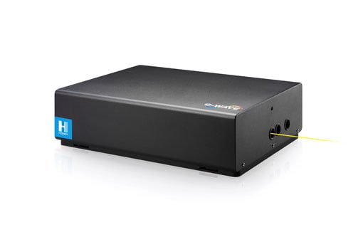
In this application note we read how the flexibility of the C-WAVE’s single frequency tunable wavelength can be utilized in nanophotonics experiments.
‘The manipulation of highly localized fi elds of surface plasmon polaritons (SPPs) forms the backbone for a vast fi eld of applications. We investigate the SPPs excited on a single crystalline gold nanoplatelet milled with a plasmonic lens structure using a scattering type scanning near fi eld optical microscope. SPPs are excited at different wavelengths in the visible regime employing a new tunable continuous wave source. Wave vector selection of the SPPs by the gold structures corresponded well with the numerically calculated dispersion relationship.’
Related products

C-WAVE Series
Widely tunable continuous-wave lasers
Wavelength: 450 nm – 1900 nm
Power: 200 mW – 1000 mW
Applications: Nanophotonics, quantum research, Raman (TERS)

