3 March, 2021
Technology leaps in quantum sensing
Advances in nano magnetometry using tailored electronics and fast-switchable lasers
Taking advantage of quantum effects has enabled the so-called first quantum revolution in the 20th century for technologies such as nuclear magnetic resonance spectroscopy, magnetic resonance imaging, and the development of transistors, LEDs, solar panels, and lasers. Today, amid the second quantum revolution new sensing schemes offer higher sensitivities and better resolution thanks to the possibility to detect and control individual quantum states in microscopic systems like atoms, quantum dots, or color centers. Emerging quantum sensing techniques could lead to the improvement of sensing technologies ranging from quantum gravitometers and accurate atomic clocks to low-noise quantum-interference microscopy and ultimately find commercial uses in gyroscopes for self-driving cars, or brain-machine interfacing via magnetic-field sensing.
As quantum sensing technology has matured over recent years, one of the contending techniques for commercially developed systems is based on nanoscale magnetometry with Nitrogen-Vacancy (NV) centers in diamond. These centers act as optically addressable, highly sensitive quantum sensors which are highly miniaturized and localized to atomic length scales. Employing a scanning-probe approach with one NV center at the tip of an AFM (Atomic Force Microscope) cantilever allows measuring magnetic fields with a spatial resolution on the nanometer scale and an extreme measurement accuracy.
Irrespective of which quantum sensing technology prevails, current solutions rely on the availability of state-of-the art components. Efforts towards commercialization drive improvement of the techniques for capturing or cooling these quantum centers and techniques for initializing, manipulating, and reading out single quantum states. This in turn drives the development of new lasers and electronics as well as miniaturization and innovative ways to allow mass production. In this white paper we give an overview of the current proposed solutions for quantum sensors based on NV center magnetometry.
Nanoscale quantum magnetometry
Over the last decade, single electron spins in diamond have been established as nanoscale quantum sensors that exhibit excellent sensitivity and nanoscale resolution for imaging and sensing of magnetic fields and other quantities, such as electric fields or temperature [1]. Spins couple naturally to magnetic fields through the Zeeman effect. They can exhibit long quantum coherence times that can be exploited to yield excellent magnetic field sensitivities. Lastly, spins can be localized to atomic length scales that, in turn, enables imaging with nanoscale resolution. These quantum sensors can measure magnetic fields, and thus, electric currents with an unprecedented sensitivity and spatial resolution. Applications include determining magnetic structures on surfaces of multiferroic or antiferromagnetic materials or mapping high-frequency currents (GHz) flowing in electronic circuits.
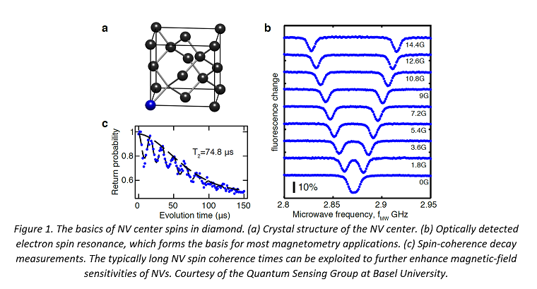
Nitrogen vacancy (NV) centers in diamond have been recently identified as suitable candidates because the point defect provides an isolated spin state which can be manipulated using microwaves. These combined properties allow for optical detection of magnetic spin resonance (ODMR) at the level of individual NV electronic spins (Fig 1). Magnetometry based on NV center spins measures the energy shifts — or, equivalently, shifts in the quantum-mechanical phase — that a spin experiences in the presence of a magnetic field. These ODMR traces represent the simplest method of implementation of such single-spin magnetometry, where the splitting between the observed ODMR resonances is directly proportional to the magnetic field the NV spin experiences.
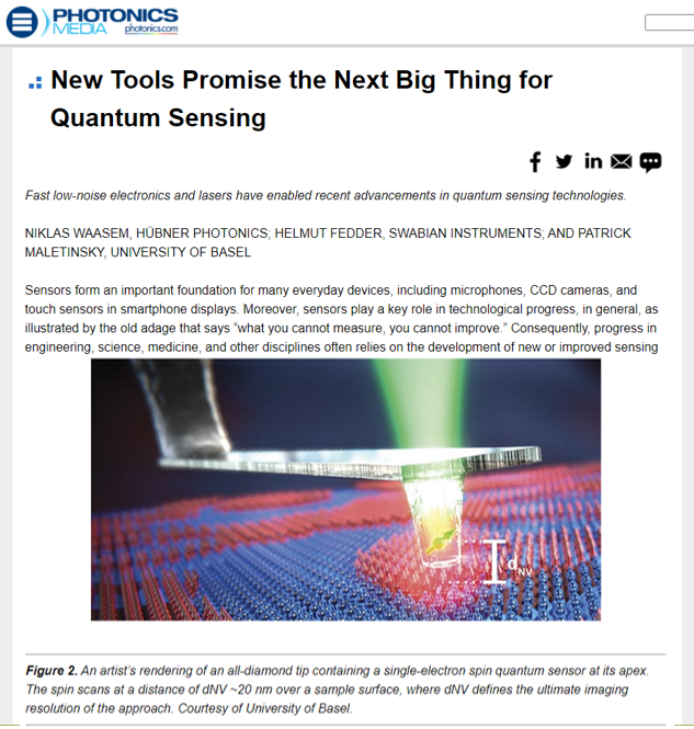
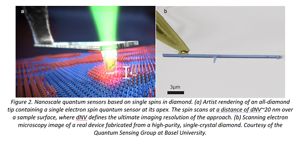
To exploit these attractive properties for nanoscale quantum sensing, the NV sensor needs to be brought in close proximity to a sensing target, ideally just a few nanometers. The most flexible approach applies a scanning probe geometry, which scans the NV and sample with respect to each other for imaging. Today, the most robust and sensitive implementation of such scanning NV magnetometry is achieved by using diamond nanopillars that contain individual NV centers at their tip as scanning probes (See Figure 2). These diamond tips allow for detection of single electron spins by stray-field imaging at resolutions around 20 nm. This approach, originally conceived in 2012 [2], has since been refined [3] to the extent that commercial solutions are available today from companies such as the Swiss startup Qnami AG.
New approach to quantum sensing
A typical quantum sensing experiment starts by initializing the NV center’s electron spin with a laser pulse lasting a few microseconds. The laser is typically operating in a wavelength range 510 – 560 nm which excites the NV center and populates a “bright” electron spin state that leads to strong fluorescence at around 638 nm when excited. By subsequently applying a microwave pulse, it is possible to flip the spin to a secondary “darker” state that shows less fluorescence. The spin-state after microwave exposure is read-out with a secondary laser pulse. The spin flip occurs when the microwave frequency matches the energy difference between the two states. As this energy difference depends on the magnetic field around the NV center, it is possible to determine the magnetic field by measuring at what microwave frequency the flipping to the darker state occurs, i.e. when the fluorescence is lowered. By applying elaborate sequences of microwave pulses of varying on/off times, so called “sensing protocols”, it is possible to maximize measurement resolution and to also assess other parameters than the magnetic field, such as electric field strengths and temperature.
Most quantum sensing experiments proceed with a parameter sweep of the interrogation time, which is often equivalent to the interpulse spacing in the sensing sequence [4]. In such cases, one sensing measurement consists of a set of pulse sequences. Companies such as Swabian Instruments have been able to apply modern single-photon counting approaches to enable fast on-the-fly processing of single-photon detection events in a flexible fashion. Such approaches eliminate common hardware limitations, such as limited histogram range and bin numbers, and greatly facilitate the implementation of novel quantum sensing schemes.
Compact fast modulated lasers
The optical initialization and the read-out sequences of the spin state of the NV-centers requires precisely tailored light pulses within the excitation spectrum of NV- centers. Other important parameters are listed in the table below:
| Wavelength | 510 nm – 560 nm |
| Modulation rise & fall time | <10 ns |
| On/off extinction ration | >60 dB |
| Beam profile | Gaussian |
| Spectral purity | >40 dB |
| Polarization extinction ratio | >100:1 |
Some quantum-sensing applications also require the ability to generate pulse trains with arbitrary on/off times and excellent intensity stability and repeatability. Until recently, the most common approach to generate such laser pulses involved the combination of a 532 nm continuous-wave laser with a double-path acousto-optical modulator (AOM). However, these laser+AOM setups are difficult to align, bulky, expensive, sensitive to shocks, and require a large or active heatsink. Since 2018, laser diodes at 515 nm with direct intensity modulation have offered an alternative solution for use in lab setups and commercial systems.
The main advantages of these laser diodes are their modulation capabilities, such as fast analogue and digital modulation with true off state, as well as precise real-time intensity control without the need for an external modulator. They also enable integration of electronics, optics, and a single-mode fiber-coupling into a compact and rugged platform. This allows user-friendly integration with quantum-sensing setups, longer lifetimes without the need for alignment or maintenance, and a more compact footprint. Figure 4 shows typical modulation characteristics of a 515-nm laser diode with a modulation frequency of 10 kHz.
Outlook
As high-purity diamond quantum sensing cantilevers emerge alongside dedicated control and measurement electronics and high-quality laser sources, the tools for versatile scanning probe quantum sensing experiments are increasingly accessible to a broader audience. Enterprises around the world have also started integrating NV based ensemble quantum sensors into commercial chip packages, with the goal of realizing the first mass produced products that leverage quantum-enhanced sensing. Further breakthroughs promise to transform quantum-sensing technologies into a versatile range of sensor products.
Download the white paper: Technology leaps in quantum sensing
References
- Chernobrod et al., Spin microscope based on optically detected magnetic resonance, J. Appl. Phys. 97, 014903 (2005).
- Maletinsky, et al., A robust scanning diamond sensor for nanoscale imaging with single nitrogen-vacancy centres, Nature Nanotechnology 7, 320 (2012).
- Hedrich et al., Parabolic diamond scanning probes for single spin magnetic field imaging, arXiv:2003.01733 (2020)
- Photonics Spectra October 2020 New Tools Promise the Next Big Thing for Quantum Sensing | Features | Oct 2020 | Photonics Spectra
Editorial: New Tools Promise the Next Big Thing for Quantum Sensing
Fast low-noise electronics and lasers have enabled recent advancements in quantum sensing technologies
The demonstration of new quantum sensing techniques and subsequent development of quantum sensing products both rely on the availability of state-of-the art components such as specialized diamond tips, suitable microscopy hardware, fast low-noise electronics, and high-performance lasers.
READ the full editorial from the October 2020 edition HERE
Authors: NIKLAS WAASEM, HÜBNER PHOTONICS; HELMUT FEDDER, SWABIAN INSTRUMENTS; AND PATRICK MALETINSKY, UNIVERSITY OF BASEL
More resources
Explore our Publications for practical insights on how our customers are leveraging the power of our lasers in their projects.
Customer publications
Product line: Cobolt
Application: Quantum
Wavelength: 532 nm, Tunable VIS
New Discovery in Quantum Technology: Shining Light on Organic Molecules
scientists have developed organic molecules that can glow brightly and be used in advanced quantum technologies
Customer publications
Product line: Cobolt
Application: Quantum
Wavelength: 594 nm, Femtosecond 1um
Nanographene Research Unveils Highly Soluble Quantum Dots
Researchers have unveiled a new family of nanographene materials with the help of the Cobolt Mambo 594 nm laser.
Customer publications
Product line: Cobolt
Application: Fluorescence microscopy
Wavelength: 488 nm
New Breakthrough in Cellular Imaging with the Cobolt 06-MLD Laser
Scientists at the KTH Royal Institute of Technology in Sweden, and Calico Life Sciences, have made significant strides in cellular imaging.


