News

Lasers for Cold Atoms and Molecules

Cooling atoms to ultralow temperatures has produced a wealth of opportunities in fundamental physics, precision metrology, and quantum science.

Laser cooling of molecular gases is challenging to implement owing to the complexity of molecular structures. Recent application of sophisticated cooling techniques to molecules has opened the door to the longstanding goal of precisely controlling molecular internal and external degrees of freedom and the resulting interaction processes. This line of research can leverage fundamental insights into how molecules interact and evolve to enable the control of reaction chemistry and the design and realization of a range of advanced quantum materials. Cold molecule gases also allow precision measurements which set a new limit for electron’s electric dipole moment and could rule out many beyond standard-model physics theories.

C-WAVE at work with trapped ions

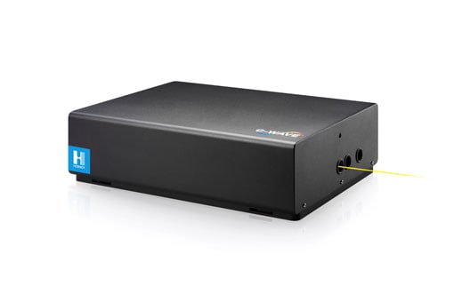
In this applications note we read how the flexibility of the C-WAVE’s single frequency tunable wavelength can be utilized for ion trapping experiments.

Coulomb crystals consisting of isotopically pure Magnesium ions are build employing a new tunable continuous-wave (cw) laser light source: Mg atoms are isotope-selective ionized by resonant two-photon excitation at a wavelength of 285.3 nm. The UV laser light is generated via resonant second-harmonic generation of the output of a new cw laser C-WAVE that offers about 0.5 W single frequency output power that is tunable in the range 450 – 650 nm. The created Mg ions are trapped and cooled, building 2D Coulomb crystals which are used for further investigation.

Download the full applications note here

Single frequency, ultra low noise lasers for atom trapping

Fiber lasers are frequently employed for trapping of cold atoms due to their high output powers, ultra-low noise level, single-frequency emission, outstanding pointing stability, nearly perfect Gaussian beam profile, and best-in-class power stability (typically < ± 0.3%  in the short and < ± 0.5% in the long term).

Related products
C-Wave

C-WAVE Series

Widely tunable continuous-wave lasers

Wavelength: 450 nm – 1900 nm
Power: 200 mW – 1000 mW
Applications: Nanophotonics, quantum research, Raman (TERS)

Read more

2024-10-18T11:41:32+02:00

Tunable lasers help in the quantum quest

The Perfect Qubit: How Tunable Light Helps in the Quantum Quest

Widely tunable continuous‐wave lasers based on OPO technology make it quicker and easier to characterize different qubit contenders

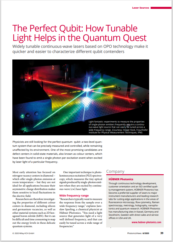
Physicists are still looking for the perfect quantum qubit: a two‐level quantum system that can be precisely measured and controlled, while remaining unaffected by its environment. One of the most promising candidates are defect centers in solid‐state materials, also known as colour centers, which have been found to emit a single photon per excitation event when excited by laser light of a particular frequency.

Download the pdf HERE

This article was written by Physics World on behalf of Hübner Photonics, and appeared in the June 2020 edition of PhotonicsViews.

Tunable lasers quantum quest

Physicists are still looking for the perfect quantum qubit: a two-level quantum system that can be precisely measured and controlled, while remaining unaffected by any changes in its environment. One of the most promising candidates are vacancy centres in solid-state materials, also known as colour centres, which have been found to emit a single photon when excited by laser light of a particular frequency.

Most early attention has focused on nitrogen vacancy centres in diamond − which offer single-photon emission at room temperature − but they are not ideal for all applications because their asymmetric charge distribution makes them sensitive to local fluctuations in the electric field. Researchers are therefore investigating the properties of different colour centres in diamond, including silicon and germanium, and other material systems such as 2D hexagonal boron nitride (hBN).

But it can be difficult and time consuming to map out the atomic-level energy transitions that generate single-photon emission in these delicate quantum systems. The most useful technique is photoluminescence excitation (PLE) spectroscopy, which measures the tiny optical signals produced by single-photon emitters when they are excited by laser light.

“Researchers typically want to measure the response from the sample over a wide frequency range,” explains Jaroslaw Sperling, a laser physicist at Hübner Photonics. “You need a light source that generates light of a very well defined frequency, and that can easily be tuned across a wide range of frequencies.”

Sperling believes that continuous-wave light sources based on optical parametric oscillators (OPOs) offer the most effective solution. Instead of the gain medium inside a conventional laser, an OPO generates coherent light from a nonlinear optical crystal pumped by a high-power laser. “OPOs first emerged about half a century ago,” says Sperling. “But commercial devices have until recently only operated in pulsed mode, since high laser powers are needed to drive the nonlinear process.”

The latest commercial systems – such as Hübner’s C-WAVE device – combine this wide tunability with the narrow linewidth needed to resolve specific resonances in the emission spectra. OPOs also offer a higher spectral purity than equivalent tunable lasers, which ensures that the weak optical signals generated by atomic-scale defects are not obscured by unwanted light emission at other wavelengths.

2024-10-03T09:29:03+02:00

Quantum sensing

Technology leaps in quantum sensing

Advances in nano magnetometry using tailored electronics and fast-switchable lasers

Taking advantage of quantum effects has enabled the so-called first quantum revolution in the 20th century for technologies such as nuclear magnetic resonance spectroscopy, magnetic resonance imaging, and the development of transistors, LEDs, solar panels, and lasers. Today, amid the second quantum revolution new sensing schemes offer higher sensitivities and better resolution thanks to the possibility to detect and control individual quantum states in microscopic systems like atoms, quantum dots, or color centers. Emerging quantum sensing techniques could lead to the improvement of sensing technologies ranging from quantum gravitometers and accurate atomic clocks to low-noise quantum-interference microscopy and ultimately find commercial uses in gyroscopes for self-driving cars, or brain-machine interfacing via magnetic-field sensing.

As quantum sensing technology has matured over recent years, one of the contending techniques for commercially developed systems is based on nanoscale magnetometry with Nitrogen-Vacancy (NV) centers in diamond. These centers act as optically addressable, highly sensitive quantum sensors which are highly miniaturized and localized to atomic length scales. Employing a scanning-probe approach with one NV center at the tip of an AFM (Atomic Force Microscope) cantilever allows measuring magnetic fields with a spatial resolution on the nanometer scale and an extreme measurement accuracy.

Irrespective of which quantum sensing technology prevails, current solutions rely on the availability of state-of-the art components. Efforts towards commercialization drive improvement of the techniques for capturing or cooling these quantum centers and techniques for initializing, manipulating, and reading out single quantum states. This in turn drives the development of new lasers and electronics as well as miniaturization and innovative ways to allow mass production. In this white paper we give an overview of the current proposed solutions for quantum sensors based on NV center magnetometry.

Nanoscale quantum magnetometry

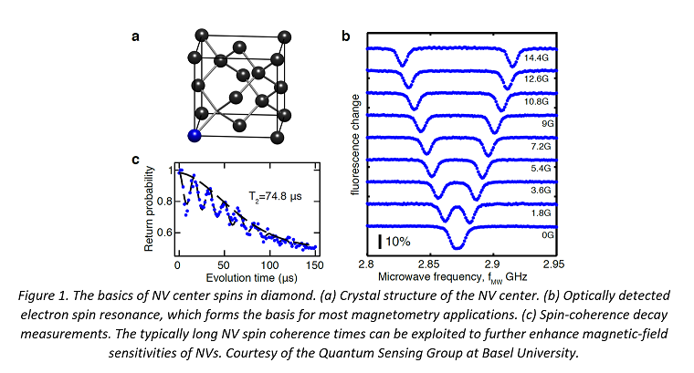
Over the last decade, single electron spins in diamond have been established as nanoscale quantum sensors that exhibit excellent sensitivity and nanoscale resolution for imaging and sensing of magnetic fields and other quantities, such as electric fields or temperature [1]. Spins couple naturally to magnetic fields through the Zeeman effect. They can exhibit long quantum coherence times that can be exploited to yield excellent magnetic field sensitivities. Lastly, spins can be localized to atomic length scales that, in turn, enables imaging with nanoscale resolution. These quantum sensors can measure magnetic fields, and thus, electric currents with an unprecedented sensitivity and spatial resolution. Applications include determining magnetic structures on surfaces of multiferroic or antiferromagnetic materials or mapping high-frequency currents (GHz) flowing in electronic circuits.

Nitrogen vacancy (NV) centers in diamond have been recently identified as suitable candidates because the point defect provides an isolated spin state which can be manipulated using microwaves. These combined properties allow for optical detection of magnetic spin resonance (ODMR) at the level of individual NV electronic spins (Fig 1). Magnetometry based on NV center spins measures the energy shifts — or, equivalently, shifts in the quantum-mechanical phase — that a spin experiences in the presence of a magnetic field. These ODMR traces represent the simplest method of implementation of such single-spin magnetometry, where the splitting between the observed ODMR resonances is directly proportional to the magnetic field the NV spin experiences.

Quantum sensing Fig 1

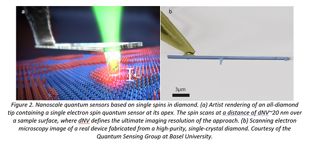
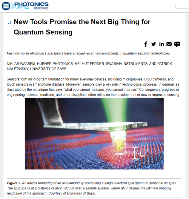
To exploit these attractive properties for nanoscale quantum sensing, the NV sensor needs to be brought in close proximity to a sensing target, ideally just a few nanometers. The most flexible approach applies a scanning probe geometry, which scans the NV and sample with respect to each other for imaging. Today, the most robust and sensitive implementation of such scanning NV magnetometry is achieved by using diamond nanopillars that contain individual NV centers at their tip as scanning probes (See Figure 2). These diamond tips allow for detection of single electron spins by stray-field imaging at resolutions around 20 nm. This approach, originally conceived in 2012 [2], has since been refined [3] to the extent that commercial solutions are available today from companies such as the Swiss startup Qnami AG.

Quantum sensing Fig 2

New approach to quantum sensing

A typical quantum sensing experiment starts by initializing the NV center’s electron spin with a laser pulse lasting a few microseconds. The laser is typically operating in a wavelength range 510 – 560 nm which excites the NV center and populates a “bright” electron spin state that leads to strong fluorescence at around 638 nm when excited. By subsequently applying a microwave pulse, it is possible to flip the spin to a secondary “darker” state that shows less fluorescence. The spin-state after microwave exposure is read-out with a secondary laser pulse. The spin flip occurs when the microwave frequency matches the energy difference between the two states. As this energy difference depends on the magnetic field around the NV center, it is possible to determine the magnetic field by measuring at what microwave frequency the flipping to the darker state occurs, i.e. when the fluorescence is lowered. By applying elaborate sequences of microwave pulses of varying on/off times, so called “sensing protocols”, it is possible to maximize measurement resolution and to also assess other parameters than the magnetic field, such as electric field strengths and temperature.

Most quantum sensing experiments proceed with a parameter sweep of the interrogation time, which is often equivalent to the interpulse spacing in the sensing sequence [4]. In such cases, one sensing measurement consists of a set of pulse sequences. Companies such as Swabian Instruments have been able to apply modern single-photon counting approaches to enable fast on-the-fly processing of single-photon detection events in a flexible fashion. Such approaches eliminate common hardware limitations, such as limited histogram range and bin numbers, and greatly facilitate the implementation of novel quantum sensing schemes.

Compact fast modulated lasers

The optical initialization and the read-out sequences of the spin state of the NV-centers requires precisely tailored light pulses within the excitation spectrum of NV- centers. Other important parameters are listed in the table below:

Wavelength 510 nm – 560 nm
Modulation rise & fall time <10 ns
On/off extinction ration >60 dB
Beam profile Gaussian
Spectral purity >40 dB
Polarization extinction ratio >100:1

Some quantum-sensing applications also require the ability to generate pulse trains with arbitrary on/off times and excellent intensity stability and repeatability. Until recently, the most common approach to generate such laser pulses involved the combination of a 532 nm continuous-wave laser with a double-path acousto-optical modulator (AOM). However, these laser+AOM setups are difficult to align, bulky, expensive, sensitive to shocks, and require a large or active heatsink. Since 2018, laser diodes at 515 nm with direct intensity modulation have offered an alternative solution for use in lab setups and commercial systems.

The main advantages of these laser diodes are their modulation capabilities, such as fast analogue and digital modulation with true off state, as well as precise real-time intensity control without the need for an external modulator. They also enable integration of electronics, optics, and a single-mode fiber-coupling into a compact and rugged platform. This allows user-friendly integration with quantum-sensing setups, longer lifetimes without the need for alignment or maintenance, and a more compact footprint. Figure 4 shows typical modulation characteristics of a 515-nm laser diode with a modulation frequency of 10 kHz.

Outlook

 As high-purity diamond quantum sensing cantilevers emerge alongside dedicated control and measurement electronics and high-quality laser sources, the tools for versatile scanning probe quantum sensing experiments are increasingly accessible to a broader audience. Enterprises around the world have also started integrating NV based ensemble quantum sensors into commercial chip packages, with the goal of realizing the first mass produced products that leverage quantum-enhanced sensing. Further breakthroughs promise to transform quantum-sensing technologies into a versatile range of sensor products.

Download the white paper: Technology leaps in quantum sensing

References

  1. Chernobrod et al., Spin microscope based on optically detected magnetic resonance, J. Appl. Phys. 97, 014903 (2005).
  2. Maletinsky, et al., A robust scanning diamond sensor for nanoscale imaging with single nitrogen-vacancy centres, Nature Nanotechnology 7, 320 (2012).
  3. Hedrich et al., Parabolic diamond scanning probes for single spin magnetic field imaging, arXiv:2003.01733 (2020)
  4. Photonics Spectra October 2020 New Tools Promise the Next Big Thing for Quantum Sensing | Features | Oct 2020 | Photonics Spectra

Editorial: New Tools Promise the Next Big Thing for Quantum Sensing

Fast low-noise electronics and lasers have enabled recent advancements in quantum sensing technologies

The demonstration of new quantum sensing techniques and subsequent development of quantum sensing products both rely on the availability of state-of-the art components such as specialized diamond tips, suitable microscopy hardware, fast low-noise electronics, and high-performance lasers.

READ the full editorial from the October 2020 edition HERE

Quantum sensing editorial

Authors: NIKLAS WAASEM, HÜBNER PHOTONICS; HELMUT FEDDER, SWABIAN INSTRUMENTS; AND PATRICK MALETINSKY, UNIVERSITY OF BASEL

2024-10-03T09:35:41+02:00

Tunable lasers for novel color centers in quantum research

How tunable lasers are helping quantum researchers search for novel color centers

In the experimental quantum research community, widely tunable continuous-wave optical parametric oscillators (CW OPOs) are gaining recognition as novel sources of tunable laser light with great potential – not least due to their unprecedented wavelength coverage. Yet, the overall experimental requirements remain often challenging for the performance of turnkey OPO devices.

Over the last few years, however, improved design techniques have yielded more sophisticated and more efficient nonlinear materials, such as periodically poled lithium niobate, that can be phase-matched to the pump laser. A new generation of continuous-wave lasers also provides higher pump powers across the frequency spectrum, making it possible for the first time to produce widely tunable CW OPOs in a turnkey system that delivers narrow-linewidth output at power levels of a few hundred milliwatts.

The advantage of OPO technology

One of the big advantages of OPO technology, compared to a conventional CW tunable laser, is that it provides more convenient control of the output wavelength. Physicists are still looking for the perfect quantum qubit: a two-level quantum system that can be precisely measured and controlled, while remaining unaffected by its environment. One of the most promising candidates are defect centres in solid-state materials, also known as colour centres, which have been found to emit a single photon per excitation event when excited by laser light of a particular frequency. Most early attention has focused on nitrogen vacancy centres in diamond − which offer single-photon emission at room temperature − but they are not ideal for all applications because their asymmetric charge distribution makes them sensitive to local fluctuations in the electric field.OPO technology also makes it easier to measure the spectra from different samples with the same experimental set-up.

Quantum researchers have been quick to recognize the benefits of continuous-wave OPOs for assessing the potential of different single-photon emitters. For example, scientists from all around the world have exploited the C-WAVE platform to measure the photoluminescence spectra from silicon, germanium and tin vacancy centres in diamond, none of which suffer from the same sensitivity to electric field as nitrogen defects.

In this webinar you will get a review of state-of-the-art CW OPO technology comprehensible even for the non-specialist, illustrated with recently published real-world experiments.

2024-10-03T09:28:59+02:00
Go to Top